
Foundation Stone Laid For First Three-Dimensional Chip Unit In Odisha
ECONOMY & POLICY

Foundation Stone Laid For First Three-Dimensional Chip Unit In Odisha

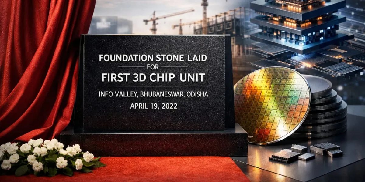
The foundation stone for the country's first advanced three-dimensional chip packaging unit was laid at Info Valley in Bhubaneswar on April nineteen, marking a significant step towards strengthening India's domestic semiconductor ecosystem and advancing the vision of Atmanirbhar Bharat in high-end electronics manufacturing. Union Minister for Electronics and IT Ashwini Vaishnaw noted that the ceremony coincided with Akshay Tritiya and expressed gratitude to the Prime Minister and the Odisha chief minister.

He indicated that the facility will use advanced three-dimensional glass substrate technology in chip manufacturing, described as a next-generation innovation in the semiconductor sector, and that the plant will be based on advanced technology rather than traditional silicon substrates. He also said authorities will pursue steps to double capacity after completion of the first phase and that several railway redevelopment projects in the state are under way to improve logistics and connectivity.

The Odisha chief minister characterised the project as a historic milestone for the state and the nation and added that global technology leaders such as Intel, Lockheed Martin and Applied Materials are associated with cutting-edge packaging technologies and have shown interest in the location. The company is reported to be investing Rs 20 billion (bn) in the first phase. The facility is expected to produce 70,000 glass panels annually, deliver 50 million (mn) assembled units and manufacture around 13,000 advanced 3DHI modules.

Officials said the project will create employment for more than 2,500 people and noted that Odisha has become the only state where both the country's first compound semiconductor fabrication unit and the first three-dimensional glass substrate packaging facility are being established. Observers view the development as likely to bolster high-end electronics manufacturing capacity in the region and to strengthen the domestic supply chain for semiconductors.

The foundation stone for the country's first advanced three-dimensional chip packaging unit was laid at Info Valley in Bhubaneswar on April nineteen, marking a significant step towards strengthening India's domestic semiconductor ecosystem and advancing the vision of Atmanirbhar Bharat in high-end electronics manufacturing. Union Minister for Electronics and IT Ashwini Vaishnaw noted that the ceremony coincided with Akshay Tritiya and expressed gratitude to the Prime Minister and the Odisha chief minister. He indicated that the facility will use advanced three-dimensional glass substrate technology in chip manufacturing, described as a next-generation innovation in the semiconductor sector, and that the plant will be based on advanced technology rather than traditional silicon substrates. He also said authorities will pursue steps to double capacity after completion of the first phase and that several railway redevelopment projects in the state are under way to improve logistics and connectivity. The Odisha chief minister characterised the project as a historic milestone for the state and the nation and added that global technology leaders such as Intel, Lockheed Martin and Applied Materials are associated with cutting-edge packaging technologies and have shown interest in the location. The company is reported to be investing Rs 20 billion (bn) in the first phase. The facility is expected to produce 70,000 glass panels annually, deliver 50 million (mn) assembled units and manufacture around 13,000 advanced 3DHI modules. Officials said the project will create employment for more than 2,500 people and noted that Odisha has become the only state where both the country's first compound semiconductor fabrication unit and the first three-dimensional glass substrate packaging facility are being established. Observers view the development as likely to bolster high-end electronics manufacturing capacity in the region and to strengthen the domestic supply chain for semiconductors.

Related Stories

Gold Stories
Next Story
Infrastructure Urban

KONE Opens India's First Digital Experience Centre in Pune

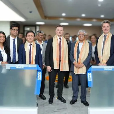
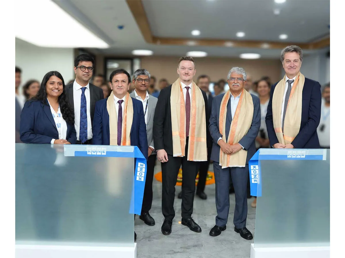
KONE, a global elevator and escalator manufacturer, has inaugurated its first Digital Experience Centre (DEC) in India, located in Pune. The facility aims to showcase how artificial intelligence (AI), connectivity and data-driven technologies can enhance customer experiences and improve building operations.The centre was inaugurated by Jussi Herlin, Executive Vice Chair, KONE Corporation; Philippe Delorme, President and CEO, KONE; and Nandan Nilekani, Co-founder and Chairman of the Board, Infosys.Designed as an interactive customer environment, the facility demonstrates digital solutions cover..
Next Story
Infrastructure Urban

CII GreenCo Launches Circularity Guidelines for Indian Industry

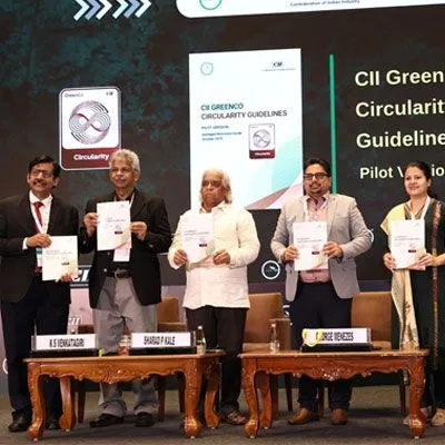
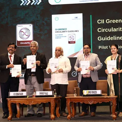
The Confederation of Indian Industry (CII) GreenCo Council has launched the CII GreenCo Circularity Guidelines – Pilot Version at the 17th CII GreenCo Waste & Resource Management Summit 2026 in Chennai. The initiative aims to strengthen resource efficiency, waste reduction and circular economy practices across Indian manufacturing and process industries.The guidelines introduce a structured framework with circularity indices covering raw materials, consumables, packaging and other resource inputs. These indicators will help industries assess existing practices, identify opportunities to ..
Next Story
Infrastructure Energy

Global Electronics Association Launches IPC-1783-CO2E Standard

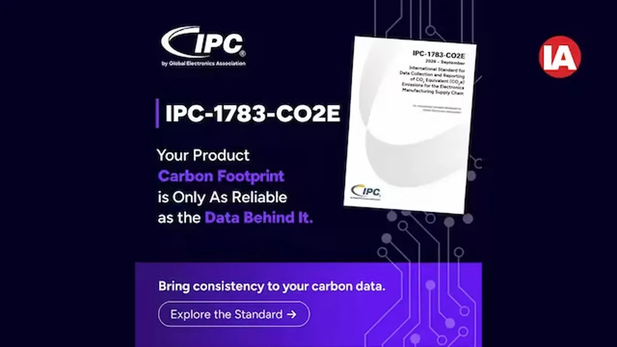
The Global Electronics Association has introduced IPC-1783-CO2E, a new international standard aimed at improving consistency, transparency and comparability in product carbon footprint reporting across the electronics manufacturing industry.The standard, titled International Standard for Data Collection and Reporting of CO2 Equivalent (CO2e) Emissions for the Electronics Manufacturing Supply Chain, provides industry-specific guidance for collecting, estimating and reporting carbon emissions data.With increasing regulatory requirements and customer expectations, electronics manufacturers face c..

Advertisement

Subscribe to Our Newsletter

Get daily newsletters around different themes from Construction world.

STAY CONNECTED

Advertisement

SPECIAL OFFER
QR Code