


India Builds Deep Semiconductor Talent for AI Era
ECONOMY & POLICY

India Builds Deep Semiconductor Talent for AI Era

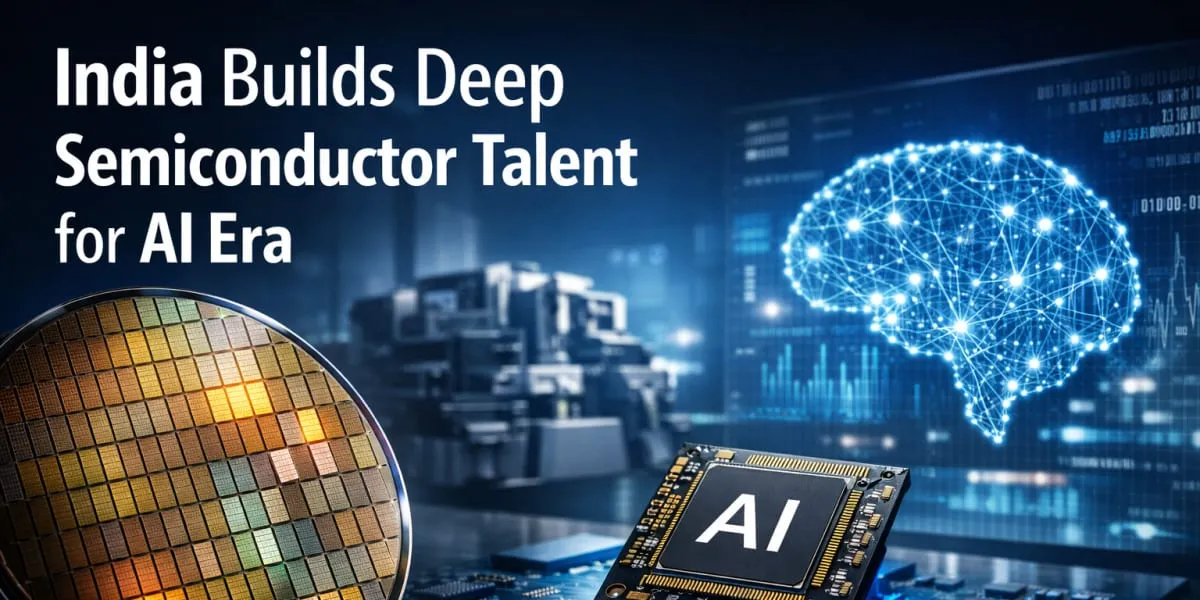
The session on semiconductor workforce in the age of artificial intelligence at the India AI Impact Summit 2026 framed talent development as the decisive link between India’s AI ambitions and its semiconductor manufacturing roadmap. The discussion brought government, industry and academic leaders together and underlined that the next phase will require a deep understanding of the fabrication ecosystem, spanning device physics, process integration and advanced manufacturing systems.

Union Minister for Electronics and Information Technology Ashwini Vaishnaw outlined a national vision to build a globally competitive semiconductor ecosystem and to strengthen India’s long-term position in the artificial intelligence value chain, noting that students across much of the country are now designing chips. S. Krishnan, Secretary, Ministry of Electronics and Information Technology (MeitY), highlighted the convergence of the India AI Mission and the India Semiconductor Mission, and said India contributes twenty per cent of the world’s semiconductor design team and has committed to 10 major semiconductor plants, with at least four set to commence production in 2026.

The panel reframed workforce development as an ecosystem challenge and argued that an industry defined by extreme precision and long learning cycles needs engineers and technicians who understand not just tool operation but process behaviour across the fabrication chain. Participants from industry and academia, including representatives from Lam Research and the Centre for Nano Science and Engineering at the Indian Institute of Science (IISc), recognised that global semiconductor hubs built capabilities over five to seven decades and that India is attempting to compress that journey.

The speakers said acceleration will be possible only through integrated collaboration between academia, equipment manufacturers and fabrication facilities, with curriculum, research and hands-on training aligned to production environments. The IISc SemiFirst collaboration with industry was cited as a model that pairs simulation-led learning with exposure to fab subsystems to ready students for operational complexity. The discussion concluded that semiconductor capability in the age of artificial intelligence depends on depth of knowledge and that building that capability at scale will be central to India’s emergence as a manufacturing and technology partner.

The session on semiconductor workforce in the age of artificial intelligence at the India AI Impact Summit 2026 framed talent development as the decisive link between India’s AI ambitions and its semiconductor manufacturing roadmap. The discussion brought government, industry and academic leaders together and underlined that the next phase will require a deep understanding of the fabrication ecosystem, spanning device physics, process integration and advanced manufacturing systems. Union Minister for Electronics and Information Technology Ashwini Vaishnaw outlined a national vision to build a globally competitive semiconductor ecosystem and to strengthen India’s long-term position in the artificial intelligence value chain, noting that students across much of the country are now designing chips. S. Krishnan, Secretary, Ministry of Electronics and Information Technology (MeitY), highlighted the convergence of the India AI Mission and the India Semiconductor Mission, and said India contributes twenty per cent of the world’s semiconductor design team and has committed to 10 major semiconductor plants, with at least four set to commence production in 2026. The panel reframed workforce development as an ecosystem challenge and argued that an industry defined by extreme precision and long learning cycles needs engineers and technicians who understand not just tool operation but process behaviour across the fabrication chain. Participants from industry and academia, including representatives from Lam Research and the Centre for Nano Science and Engineering at the Indian Institute of Science (IISc), recognised that global semiconductor hubs built capabilities over five to seven decades and that India is attempting to compress that journey. The speakers said acceleration will be possible only through integrated collaboration between academia, equipment manufacturers and fabrication facilities, with curriculum, research and hands-on training aligned to production environments. The IISc SemiFirst collaboration with industry was cited as a model that pairs simulation-led learning with exposure to fab subsystems to ready students for operational complexity. The discussion concluded that semiconductor capability in the age of artificial intelligence depends on depth of knowledge and that building that capability at scale will be central to India’s emergence as a manufacturing and technology partner.

Next Story
Infrastructure Urban

Panasonic Showcases Connected Display Solutions

Panasonic Life Solutions India showcased its integrated display, projection, broadcast and communication technologies at Panasonic Tech Summit 2026 in New Delhi. Hosted through its System Solutions Division, the two-day event highlighted connected technology solutions for education, healthcare, retail, transportation, corporate offices and entertainment.The summit, themed ‘Turning Technology into Value’, featured experience-led zones covering QSR, retail, transit, corporate offices, healthcare, education, security, projection, home theatre and professional displays. Panasonic also introduc..

Next Story
Infrastructure Transport

Kapsch to Deliver India’s First C-ITS Project

"Kapsch TrafficCom will deliver India’s first Cooperative Intelligent Transport Systems project on a key expressway near New Delhi. The project will be implemented with Superwave Communication And Infrasolution Limited to demonstrate how connected mobility can improve road safety and traffic efficiency.The pilot will use real-time connectivity and AI-enabled situational awareness to support road users, especially in high-risk areas such as temporary work zones. Drivers will receive alerts on roadworks, maintenance vehicles, hazardous locations, traffic queues and temporary virtual signage di..

Next Story
Infrastructure Urban

Eurobond Net Profit Rises 44 Per Cent

Euro Panel Products, the parent company of Eurobond, reported a 44.13 per cent year-on-year rise in net profit for FY25–26. The company’s revenue from operations grew 18.91 per cent to Rs 503.20 crore, compared to Rs 423.18 crore in the previous financial year.The company’s full-year EBITDA stood at Rs 56.67 crore, marking a 31.82 per cent increase. Profit after tax rose to Rs 26.56 crore, while net worth increased 20.15 per cent to Rs 160.07 crore. Earnings per share for the year stood at Rs 10.84.Divyam Rajesh Shah, Whole Time Director and CFO, Euro Panel Products, said the company’s..

Advertisement

Subscribe to Our Newsletter

Get daily newsletters around different themes from Construction world.

STAY CONNECTED

Advertisement

Advertisement

Advertisement

-->