


Henkel Opens Electronics Co-Innovation Hub in Bengaluru
Interiors

Henkel Opens Electronics Co-Innovation Hub in Bengaluru

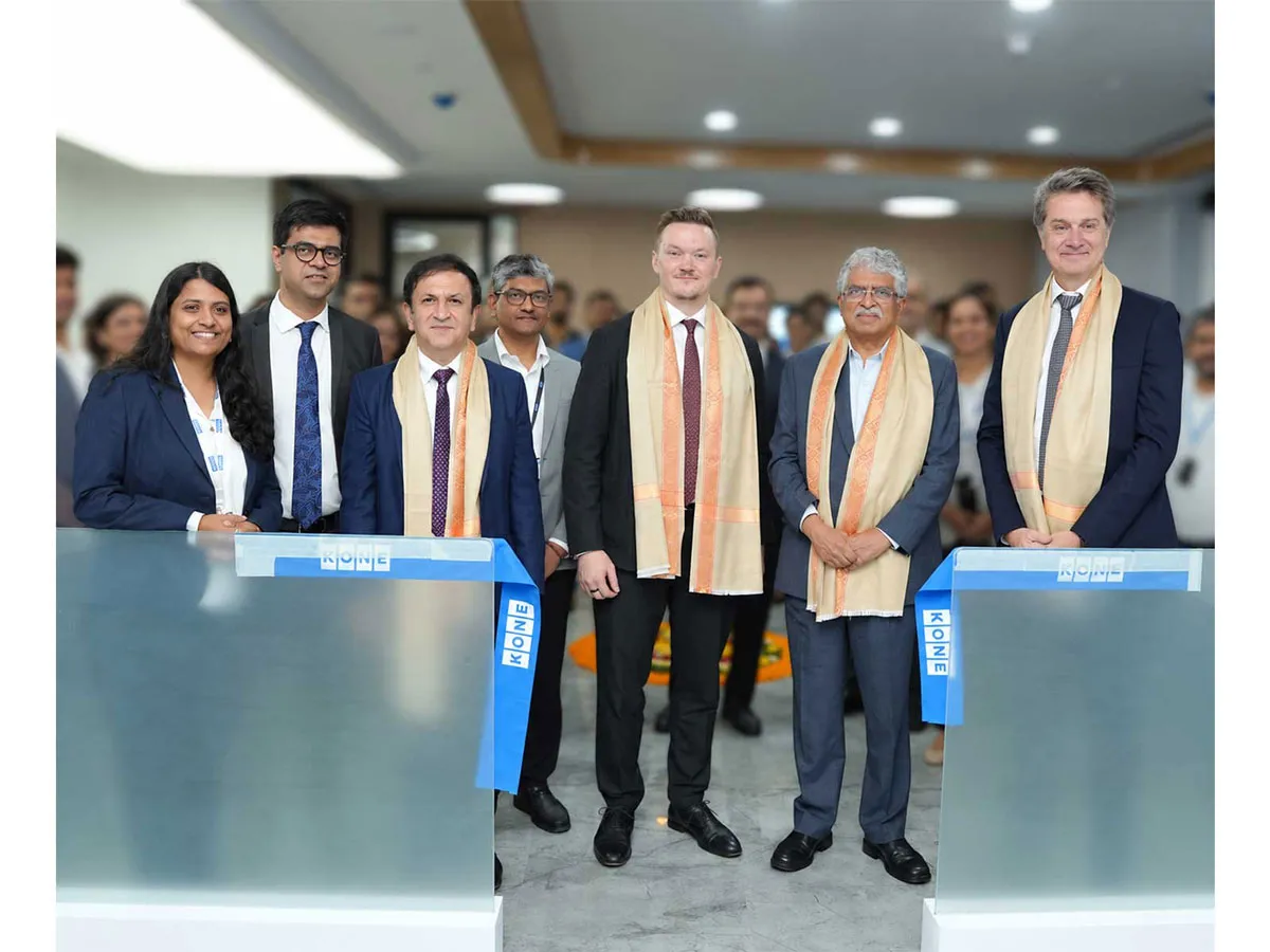
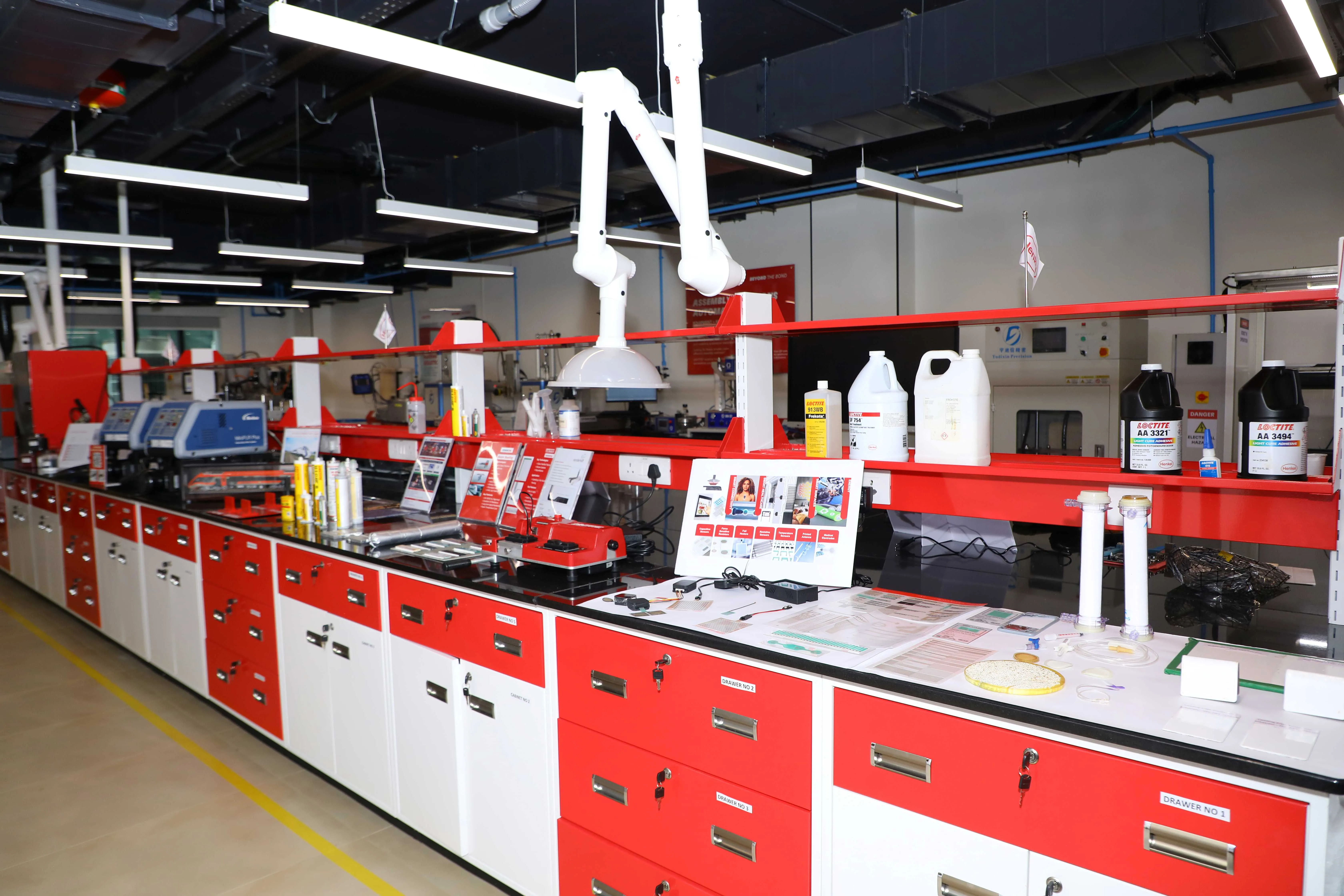
Henkel has launched a Customer Application Center in Bengaluru, aimed at supporting India’s growing electronics manufacturing sector through co-development, testing and validation of advanced materials.

The facility marks a significant application engineering investment for Henkel in the India Middle East and Africa region and addresses the lack of localised testing and validation infrastructure. It enables manufacturers to develop and scale advanced adhesive and thermal management solutions without relying on overseas facilities.

India’s electronics manufacturing sector has expanded nearly six-fold over the past decade, driven by growth in data centres, AI computing, 5G infrastructure, electric vehicle systems, industrial automation and medical devices. These sectors require high-performance materials and faster, localised engineering support.

“India's electronics manufacturing ecosystem is at an inflection point, and Bengaluru is at the center of it,” said S. Sunil Kumar, Country President – India, Henkel. “What manufacturers across our focus sectors increasingly need is not just world-class materials, but a local partner who can co-develop, test, and validate those materials under real production conditions, and help them move from concept to market faster. That is precisely what this center is designed to do. It is our most tangible expression yet of Henkel's long-term commitment to India's electronics future.”

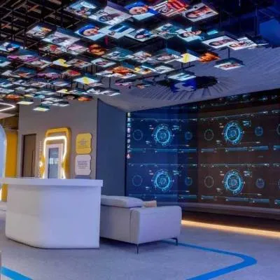
The 5,000 sq ft facility includes around 2,400 sq ft of laboratory and testing space designed to replicate manufacturing conditions. It supports sectors such as telecom, data centres, EV systems, industrial automation and medical electronics, with capabilities spanning thermal testing, dispensing systems, electrical characterisation and rapid curing.

The centre is expected to enable localised application engineering, process optimisation and validation, reducing development timelines and supporting India’s manufacturing initiatives.

Photo caption: Advanced electronics lab bridging materials and applications at Henkel Adhesive Technologies’ Customer Application Center in Bengaluru

Henkel has launched a Customer Application Center in Bengaluru, aimed at supporting India’s growing electronics manufacturing sector through co-development, testing and validation of advanced materials. The facility marks a significant application engineering investment for Henkel in the India Middle East and Africa region and addresses the lack of localised testing and validation infrastructure. It enables manufacturers to develop and scale advanced adhesive and thermal management solutions without relying on overseas facilities. India’s electronics manufacturing sector has expanded nearly six-fold over the past decade, driven by growth in data centres, AI computing, 5G infrastructure, electric vehicle systems, industrial automation and medical devices. These sectors require high-performance materials and faster, localised engineering support. “India's electronics manufacturing ecosystem is at an inflection point, and Bengaluru is at the center of it,” said S. Sunil Kumar, Country President – India, Henkel. “What manufacturers across our focus sectors increasingly need is not just world-class materials, but a local partner who can co-develop, test, and validate those materials under real production conditions, and help them move from concept to market faster. That is precisely what this center is designed to do. It is our most tangible expression yet of Henkel's long-term commitment to India's electronics future.” The 5,000 sq ft facility includes around 2,400 sq ft of laboratory and testing space designed to replicate manufacturing conditions. It supports sectors such as telecom, data centres, EV systems, industrial automation and medical electronics, with capabilities spanning thermal testing, dispensing systems, electrical characterisation and rapid curing. The centre is expected to enable localised application engineering, process optimisation and validation, reducing development timelines and supporting India’s manufacturing initiatives.Photo caption: Advanced electronics lab bridging materials and applications at Henkel Adhesive Technologies’ Customer Application Center in Bengaluru

Next Story
Infrastructure Urban

Dreamfly Named Among 100 Desi Deeptechs

Dreamfly Innovations has been recognised among the ‘100 Desi Deeptechs’, an initiative by Startup Policy Forum in collaboration with MeitY Startup Hub, Startup India and Indian Institute of Technology Madras. The initiative highlights founders and companies building core technologies critical to India’s long-term growth and self-reliance.The cohort includes startups working across drones and aerospace, defence technology, cleantech, robotics, semiconductors, advanced manufacturing and electric mobility. It aims to bring deeptech founders and policymakers together to strengthen India’s ..

Next Story
Infrastructure Urban

Vedanta Secures AA+ Rating from ICRA

Vedanta Group has received its highest domestic credit rating in over a decade after ICRA upgraded the long-term ratings of Vedanta Limited and Vedanta Aluminium Metal Limited to AA+ with a Stable outlook. Talwandi Sabo Power Limited was also upgraded to AA-/Stable from A+/Watch Developing, while the group’s short-term rating was reaffirmed at A1+.The rating action marks Vedanta’s highest domestic credit rating since 2014. Vedanta Limited and Vedanta Aluminium Metal Limited, two of the largest entities emerging from the demerger, together account for over 75 per cent of the group’s long-..

Next Story
Infrastructure Urban

Netrasemi Launches Edge AI Chip A2000

Fabless semiconductor startup Netrasemi has launched its flagship Edge AI system-on-chip, A2000, after achieving successful silicon bring-up. Fabricated at TSMC’s 12 nm technology node, the chip is designed for on-device AI, smart vision, real-time video analytics and secure edge computing.A2000 features Netrasemi’s in-house Neural Processing Unit, Vision Processing Unit, Image Signal Processor, crypto engines and other hardware acceleration IP cores. It also uses the company’s patented heterogeneous graph-stream parallel processing architecture.The chip targets applications such as smar..

Advertisement

Subscribe to Our Newsletter

Get daily newsletters around different themes from Construction world.

STAY CONNECTED

Advertisement

Advertisement

Advertisement

-->