India Opens First 3nm Chip Design Centre
Technology

India Opens First 3nm Chip Design Centre

Union Minister for Electronics & IT, Railways, and Information & Broadcasting, Shri Ashwini Vaishnaw, today inaugurated two advanced semiconductor design facilities of Renesas Electronics India Private Limited, located in Noida and Bengaluru. Marking a milestone in India's semiconductor journey, the Minister announced that these centres include the country’s first-ever facility dedicated to designing next-generation 3 nanometre (nm) chips.

“Designing at 3nm is truly cutting-edge. India has already worked on 7nm and 5nm nodes, but this takes us into a new league,” said Shri Vaishnaw, highlighting the significance of the new centre in the global semiconductor landscape.

He also outlined India’s comprehensive semiconductor strategy, which spans design, fabrication, ATMP (Assembly, Testing, Marking, and Packaging), equipment, and material supply chains. Citing recent industry confidence at global events like Davos, he noted major investments from firms such as Applied Materials and Lam Research.

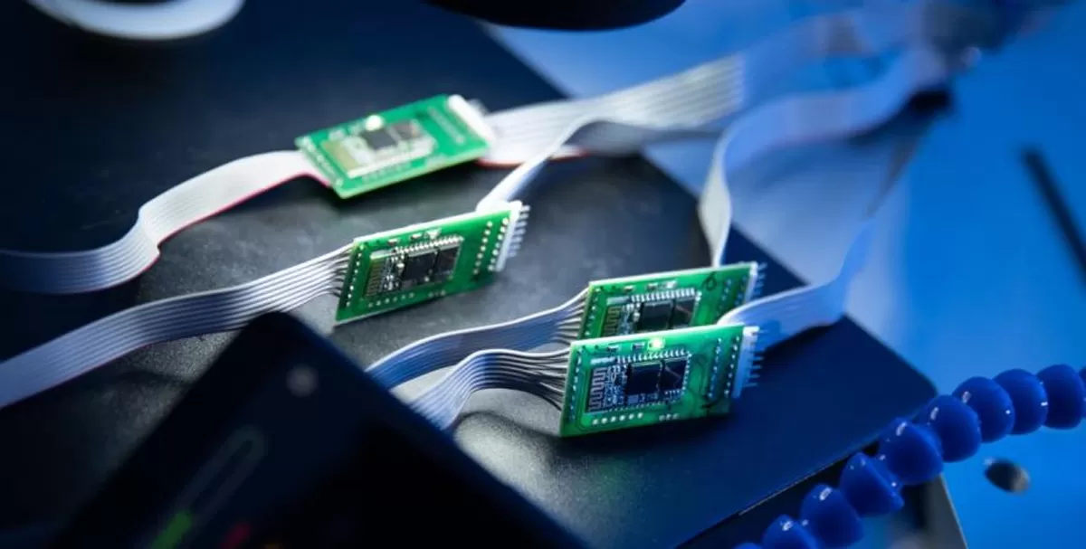
To nurture talent, Shri Vaishnaw announced a new semiconductor learning kit for engineering students to enhance practical skills. Over 270 academic institutions that have received advanced Electronic Design Automation (EDA) tools under the India Semiconductor Mission will now also benefit from these hands-on hardware kits. “We are developing not just infrastructure, but future-ready engineers,” he added.

The Minister commended CDAC and the ISM team for their swift implementation and credited Prime Minister Narendra Modi’s strategic focus on semiconductors under the Aatmanirbhar Bharat initiative. “In just three years, India’s semiconductor sector has evolved from an idea to a global force,” he stated, adding that booming demand across smartphones, laptops, medical devices, defence, and automotive sectors makes this progress timely.

Renesas CEO & MD Shri Hidetoshi Shibata called India a “strategic cornerstone” for the company. He reaffirmed Renesas’ commitment to building end-to-end semiconductor capabilities in India, from architecture to testing, and to supporting over 250 academic institutions and numerous startups through schemes such as Chips to Startup (C2S) and the Design Linked Incentive (DLI) Scheme.

He emphasised that India’s engineering talent and Indo-Japan cooperation would help redefine the global semiconductor ecosystem.

Union Minister for Electronics & IT, Railways, and Information & Broadcasting, Shri Ashwini Vaishnaw, today inaugurated two advanced semiconductor design facilities of Renesas Electronics India Private Limited, located in Noida and Bengaluru. Marking a milestone in India's semiconductor journey, the Minister announced that these centres include the country’s first-ever facility dedicated to designing next-generation 3 nanometre (nm) chips.“Designing at 3nm is truly cutting-edge. India has already worked on 7nm and 5nm nodes, but this takes us into a new league,” said Shri Vaishnaw, highlighting the significance of the new centre in the global semiconductor landscape.He also outlined India’s comprehensive semiconductor strategy, which spans design, fabrication, ATMP (Assembly, Testing, Marking, and Packaging), equipment, and material supply chains. Citing recent industry confidence at global events like Davos, he noted major investments from firms such as Applied Materials and Lam Research.To nurture talent, Shri Vaishnaw announced a new semiconductor learning kit for engineering students to enhance practical skills. Over 270 academic institutions that have received advanced Electronic Design Automation (EDA) tools under the India Semiconductor Mission will now also benefit from these hands-on hardware kits. “We are developing not just infrastructure, but future-ready engineers,” he added.The Minister commended CDAC and the ISM team for their swift implementation and credited Prime Minister Narendra Modi’s strategic focus on semiconductors under the Aatmanirbhar Bharat initiative. “In just three years, India’s semiconductor sector has evolved from an idea to a global force,” he stated, adding that booming demand across smartphones, laptops, medical devices, defence, and automotive sectors makes this progress timely.Renesas CEO & MD Shri Hidetoshi Shibata called India a “strategic cornerstone” for the company. He reaffirmed Renesas’ commitment to building end-to-end semiconductor capabilities in India, from architecture to testing, and to supporting over 250 academic institutions and numerous startups through schemes such as Chips to Startup (C2S) and the Design Linked Incentive (DLI) Scheme.He emphasised that India’s engineering talent and Indo-Japan cooperation would help redefine the global semiconductor ecosystem.

Next Story
Technology

Building Faster, Smarter, and Greener!

Backed by ULCCS’s century-old legacy, U-Sphere combines technology, modular design and sustainable practices to deliver faster and more efficient projects. In an interaction with CW, Rohit Prabhakar, Director - Business Development, shares how the company’s integrated model of ‘Speed-Build’, ‘Smart-Build’ and ‘Sustain-Build’ is redefining construction efficiency, quality and environmental responsibility in India.U-Sphere positions itself at the intersection of speed, sustainability and smart design. How does this translate into measurable efficiency on the ground?At U..

Next Story
Infrastructure Transport

Smart Roads, Smarter India

India’s infrastructure boom is not only about laying more kilometres of highways – it’s about building them smarter, safer and more sustainably. From drones mapping fragile Himalayan slopes to 3D machine-controlled graders reducing human error, technology is steadily reshaping the way projects are planned and executed. Yet, the journey towards digitisation remains complex, demanding not just capital but also coordination, training and vision.Until recently, engineers largely depended on Survey of India toposheets and traditional survey methods like total stations or DGPS to prepare detai..

Next Story
Real Estate

What Does DCPR 2034 Mean?

The Maharashtra government has eased approval norms for high-rise buildings under DCPR 2034, enabling the municipal commissioner to sanction projects up to 180 m on large plots. This change is expected to streamline approvals, reduce procedural delays and accelerate redevelopment, drawing reactions from developers, planners and industry experts about its implications for Mumbai’s vertical growth.Under the revised DCPR 2034 rules, buildings on plots of 2,000 sq m or more can now be approved up to 180 m by the municipal commissioner, provided structural and geotechnical reports are certified b..

Advertisement

Subscribe to Our Newsletter

Get daily newsletters around different themes from Construction world.

STAY CONNECTED

Advertisement

Advertisement

Advertisement

Talk to us?