India is Democratising Chip Design for a Self-Reliant Future


Pecan Realty Completes Rs 1.5 Billion Transactions
Pecan Realty has recently completed four institutional transactions worth over Rs 1.5 billion over the past two years, strengthening its position as an execution-led real estate platform. The deals include resolution-led acquisitions, structured finance transactions and capital partnerships across its development portfolio.The transactions covered acquisitions through the National Company Law Tribunal process and helped provide repayment or exits to both private and public sector lenders. The company said the deals demonstrate its ability to resolve complex project situations, work with instit..
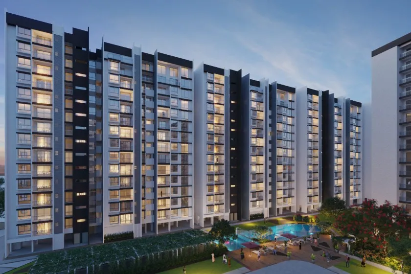
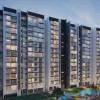
SNN Estates Expands North Bengaluru Housing Project
SNN Estates has announced an expansion of its SNN Estates Felicity residential project in North Bengaluru following strong buyer demand, with 75 per cent of the first-phase inventory sold within three days of launch.The developer will add 76 apartments in the new phase, taking the project's estimated revenue potential to around Rs 1,000 crore upon completion of Phase 2.Spread across 6.5 acres in Rachenahalli, near Manyata Tech Park, the project comprises 604 apartments in 1.5, 2, 2.5, 3 and 4 BHK configurations. The development includes a 50,000-sq-ft clubhouse with amenities such as sports co..

SCG Drives ASEAN Industrial Transformation Strategy
SCG is strengthening its focus on ASEAN as a key growth region by advancing industrial transformation, enhancing competitiveness and building resilient regional value chains. Thammasak Sethaudom, President and Chief Executive Officer, SCG, highlighted the need for industries to continuously develop capabilities, strengthen resilience and deepen regional cooperation to achieve sustainable long-term growth.SCG views ASEAN as an important growth engine alongside China, supported by favourable demographics, trade connectivity and investment flows. With ASEAN’s GDP projected to grow by around 4.7..
Latest Updates