
+
Finance Ministry Clears Rs One Point Two Five Trillion for ISM
ROADS & HIGHWAYS

Finance Ministry Clears Rs One Point Two Five Trillion for ISM

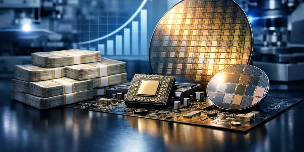
The expenditure department of the Finance Ministry has cleared an allocation of Rs one point two five trillion (tn) for India Semiconductor Mission two point zero, surpassing the Rs 760 billion (bn) outlay for ISM one point zero. The move is intended to advance the country's chip-making ambitions and to position India as a global semiconductor destination. The package will focus on equipment, materials, indigenous designs and resilient supply chains.

The Expenditure Finance Committee has approved the proposal and it will be placed before the Cabinet for final sanction. The second edition of the India Semiconductor Mission was announced in the Union Budget for 2026-27 with the objective of promoting a comprehensive chip manufacturing ecosystem covering machinery, inputs and intellectual property. Officials view ISM two point zero as a signal of sustained commitment to build domestic capability and attract ecosystem partners.

Union Minister for Electronics and IT Ashwini Vaishnaw has indicated that ISM two point zero will prioritise indigenous chip design, productisation, partner attraction and talent development. To date, 12 semiconductor manufacturing projects have been approved with an investment pipeline of about Rs one point six four trillion (tn), including one fabrication unit, two compound semiconductor fabrication units and nine packaging units. On the design front, 24 projects are supported under the Design Linked Incentive Scheme, 105 companies have been assisted with advanced chip design tools and 23 design tapeouts have been completed at various foundries.

A senior official in the IT Ministry said two of the approved projects have entered commercial manufacture earlier this year and that another facility was expected to be inaugurated soon, with further projects anticipated before the end of the calendar year. The official characterised the developments as the realisation of a long-held national objective to establish commercial semiconductor manufacturing in India. Observers note that the country is strengthening its position in the global technology landscape and in standards discussions.

The expenditure department of the Finance Ministry has cleared an allocation of Rs one point two five trillion (tn) for India Semiconductor Mission two point zero, surpassing the Rs 760 billion (bn) outlay for ISM one point zero. The move is intended to advance the country's chip-making ambitions and to position India as a global semiconductor destination. The package will focus on equipment, materials, indigenous designs and resilient supply chains. The Expenditure Finance Committee has approved the proposal and it will be placed before the Cabinet for final sanction. The second edition of the India Semiconductor Mission was announced in the Union Budget for 2026-27 with the objective of promoting a comprehensive chip manufacturing ecosystem covering machinery, inputs and intellectual property. Officials view ISM two point zero as a signal of sustained commitment to build domestic capability and attract ecosystem partners. Union Minister for Electronics and IT Ashwini Vaishnaw has indicated that ISM two point zero will prioritise indigenous chip design, productisation, partner attraction and talent development. To date, 12 semiconductor manufacturing projects have been approved with an investment pipeline of about Rs one point six four trillion (tn), including one fabrication unit, two compound semiconductor fabrication units and nine packaging units. On the design front, 24 projects are supported under the Design Linked Incentive Scheme, 105 companies have been assisted with advanced chip design tools and 23 design tapeouts have been completed at various foundries. A senior official in the IT Ministry said two of the approved projects have entered commercial manufacture earlier this year and that another facility was expected to be inaugurated soon, with further projects anticipated before the end of the calendar year. The official characterised the developments as the realisation of a long-held national objective to establish commercial semiconductor manufacturing in India. Observers note that the country is strengthening its position in the global technology landscape and in standards discussions.

Related Stories

Gold Stories

Next Story
Infrastructure Transport

MMRDA Targets Completion of Projects by December 2028

The Mumbai Metropolitan Region Development Authority (MMRDA) is targeting the completion of all its ongoing infrastructure projects by December 2028, a year ahead of its December 2029 deadline, Metropolitan Commissioner Dr Sanjay Mukherjee has said.Speaking at the sixth edition of the Real Estate & Infrastructure Investors' Summit (REIIS) 2026 in Mumbai, Mukherjee said the authority was developing an integrated network of roads, tunnels, sea links and Metro corridors under its broader vision of “Mumbai in 59 Minutes”.The objective is to improve east-west and north-south connectivity an..

Next Story
Building Material

High-Performance Façades Gain Ground in Indian Buildings

High-performance façades are gaining greater importance in Indian architecture as developers and architects increasingly focus on energy efficiency, thermal comfort and building performance, according to Shankar Fenestrations & Glasses.The company said modern façade systems are increasingly being considered as part of a building's overall performance strategy rather than being used primarily as aesthetic elements.High-performance glass, curtain wall systems and structural glazing can contribute to thermal regulation, solar control, daylight management and indoor comfort. Their growing ad..

Next Story
Technology

SPML Infra's 104.4 kWh BESS Battery Pack Clears Global Tests

SPML Infra has announced that its proprietary 104.4 kWh Battery Energy Storage System (BESS) battery pack has completed key international safety, performance and transportation testing and certification requirements, marking a step towards its commercial deployment.Developed under the company's own intellectual property, the battery pack has completed requirements under UL9540A, IEC 62619, IEC 63056, IEC 60730, IEC 61000-6-2, IEC 61000-6-4 and UN38.3 standards.The testing covers areas including thermal runaway safety, battery performance, system functional safety, electromagnetic compatibility..

Advertisement

Subscribe to Our Newsletter

Get daily newsletters around different themes from Construction world.

STAY CONNECTED

Advertisement

SPECIAL OFFER
QR Code