
India Emerges As Global Hub For Semiconductor Design And R&D
ECONOMY & POLICY

India Emerges As Global Hub For Semiconductor Design And R&D

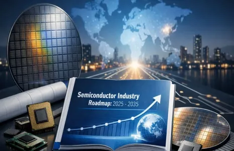
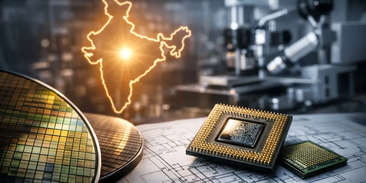
India has emerged as a global hub for semiconductor design and R&D, with government policy inspired by the Prime Minister's vision of Atmanirbhar Bharat and Make in India, Make for the world. The strategy aims to build an ecosystem covering R&D, design, fabrication, assembly, testing, packaging and module manufacturing and talent development. In three years the Semicon India Programme has attracted investment commitments of about Rs one point six trillion (tn).

The Programme has approved ten units including two fabs and eight ATMPs or OSATs with construction progressing rapidly. One unit has started commercial production and three units are in pilot production, while most approved projects include pilot lines and some have dedicated R&D activity.

24 projects for chip and SoC design have been approved with a total project value of Rs nine billion (bn), addressing sectors such as video surveillance, drone detection, energy metering, microprocessors, satellite communications and broadband and IoT SoCs. 14 companies have secured venture capital and Indian startups have raised Rs six point five bn in VC funding. Seven chips have been fabricated out of 16 taped out designs across multiple foundries including advanced 12 nm nodes at TSMC.

105 fabless design companies have been supported with access to advanced infrastructure, consuming six million (mn) hours of tool usage, and 315 universities have accessed EDA tools with usage exceeding 18.5 mn hours. 146 designs have been taped out by 49 institutions and SCL has fabricated and packaged 94 student designed chips. These measures aim to strengthen design capability and deepen academic engagement in semiconductor innovation.

Union Budget 2026-27 announced India Semiconductor Mission 2.0 to support equipment, materials, full stack design and Indian IP. ANRF has an outlay of Rs 500 bn and the RDI Fund has Rs one tn to support research through to commercialisation, while MeitY supports AMOLED displays with Rs 420 mn and a GaN initiative with Rs three point three four bn.

India has emerged as a global hub for semiconductor design and R&D, with government policy inspired by the Prime Minister's vision of Atmanirbhar Bharat and Make in India, Make for the world. The strategy aims to build an ecosystem covering R&D, design, fabrication, assembly, testing, packaging and module manufacturing and talent development. In three years the Semicon India Programme has attracted investment commitments of about Rs one point six trillion (tn). The Programme has approved ten units including two fabs and eight ATMPs or OSATs with construction progressing rapidly. One unit has started commercial production and three units are in pilot production, while most approved projects include pilot lines and some have dedicated R&D activity. 24 projects for chip and SoC design have been approved with a total project value of Rs nine billion (bn), addressing sectors such as video surveillance, drone detection, energy metering, microprocessors, satellite communications and broadband and IoT SoCs. 14 companies have secured venture capital and Indian startups have raised Rs six point five bn in VC funding. Seven chips have been fabricated out of 16 taped out designs across multiple foundries including advanced 12 nm nodes at TSMC. 105 fabless design companies have been supported with access to advanced infrastructure, consuming six million (mn) hours of tool usage, and 315 universities have accessed EDA tools with usage exceeding 18.5 mn hours. 146 designs have been taped out by 49 institutions and SCL has fabricated and packaged 94 student designed chips. These measures aim to strengthen design capability and deepen academic engagement in semiconductor innovation. Union Budget 2026-27 announced India Semiconductor Mission 2.0 to support equipment, materials, full stack design and Indian IP. ANRF has an outlay of Rs 500 bn and the RDI Fund has Rs one tn to support research through to commercialisation, while MeitY supports AMOLED displays with Rs 420 mn and a GaN initiative with Rs three point three four bn.

Next Story
Real Estate

LML Realty Launches Cinema Campaign on Industrial Vision

LML Realty has launched a cinema advertising campaign in partnership with PVR INOX across 81 screens in Gurugram and Faridabad, showcasing the brand’s transformation from a mobility icon to an industrial infrastructure developer.The campaign features a cinematic brand film tracing LML’s journey since 1972, beginning with its iconic scooters and highlighting its evolution into creating infrastructure solutions that support India’s manufacturing growth.The film focuses on LML Industrial Park at Jhirka Valley, the company’s flagship industrial development approved under the Haryana Govern..

Next Story
Real Estate

IIM Ahmedabad Publishes Case Study on HoABL’s Business Model

The Indian Institute of Management Ahmedabad (IIMA) has published a case study on The House of Abhinandan Lodha (HoABL), examining the company’s digital-first consumer journey and business model that created India’s branded land category.Titled “HoABL: Ready for Scaling Up”, the case study has been published by the IIMA Case Centre and co-authored by Sourav Borah, Associate Professor of Marketing at IIMA, and Dr Aparna Kansal of IMT Ghaziabad. IIMA case studies are used across management and executive education programmes to help students and business leaders analyse strategic decision..

Next Story
Infrastructure Energy

Advait Energy and MEIL Partner for Energy Transition Projects

Advait Energy Transitions Limited (AETL) and Manipal Energy Infratech Limited (MEIL), a company of The Manipal Group, have entered into a strategic Memorandum of Understanding (MoU) to collaborate on power and energy transition opportunities across India and international markets.The partnership aims to combine AETL’s expertise in innovative energy technologies and manufacturing with MEIL’s EPC execution capabilities and project management experience. The collaboration will focus on opportunities across Power Transmission & Distribution, Renewable Energy, Battery Energy Storage Systems..

Advertisement

Subscribe to Our Newsletter

Get daily newsletters around different themes from Construction world.

STAY CONNECTED

Advertisement

Advertisement

Advertisement