NITI Aayog Sets US Dollar 120-150 bn Semiconductor Target

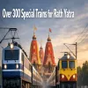
Railways To Operate Over 300 Special Trains For Rath Yatra
Union Railway Minister Ashwini Vaishnaw announced that Indian Railways (IR) will operate more than 300 special trains for the annual Jagannath Rath Yatra in Odisha and over 100 special trains during the Onam festival in Keralam. He flagged off the Nanded–Mumbai and Tanakpur–Nanded Express trains and inaugurated the extension of the Tanakpur–Pilibhit service up to Shahjahanpur via video conference from Rail Sadan in Bhubaneswar. He noted that the summer season, which concluded on 30 June, had seen a record 15,000 special trains. Vaishnaw stated that the newly launched services are intende..

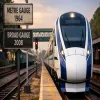
Vande Bharat Express To Start From Tripura Soon
Tripura Chief Minister Manik Saha said the Vande Bharat Express will commence operations from Tripura in the coming days after he flagged off the Agartala–Karimganj MEMU service at Agartala Railway Station. He recalled the rail history of the state, noting that a metre-gauge service first arrived in 1964 and that broad gauge reached Agartala in 2008 following national projects and later upgrades under the Act East policy. The event was described as a milestone for regional connectivity and the MEMU was presented as the first electric passenger train to originate from Tripura.\n\nSaha said he..
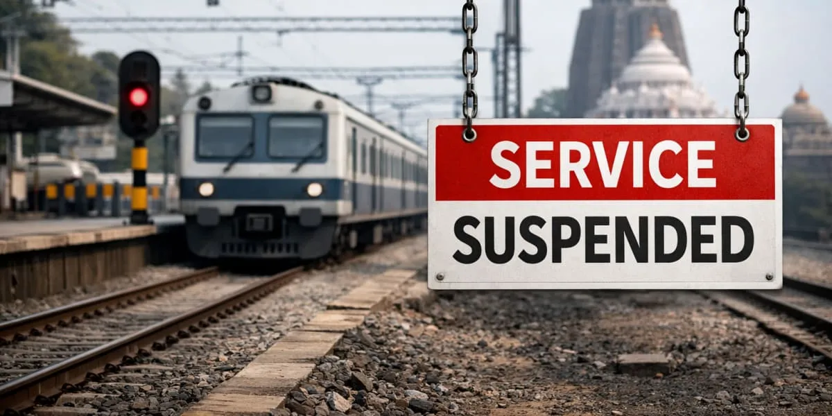
MEMU Suspension Disrupts Commuters Between Vadodara And Dahod
The Vadodara–Dahod Mainline Electric Multiple Unit (MEMU) service has been temporarily suspended for 26 days after its rake was diverted to Odisha to manage the surge in passenger traffic during the annual Rath Yatra in Puri. Indian Railways redeployed several MEMU rakes from different zones to meet the additional travel demand for the festival scheduled from the seventh of July to the second of August. As a result, train numbers 69233 and 69234 operating between Vadodara and Dahod will remain cancelled for the duration. Railway authorities advised passengers to use alternative train service..
Latest Updates